Укладка чипов боком Дает ИИ Больше Памяти
Графическим процессорам и другим мощным процессорам искусственного интеллекта просто не хватает памяти. Современные компьютеры для центров обработки данных используют 12-разрядную память. Но по мере того, как производители памяти пытаются увеличить количество стеков, чтобы вместить больше битов и увеличить пропускную способность, эксперты опасаются, что память с высокой пропускной способностью (HBM) будет накапливать достаточно тепла, чтобы сгореть дотла. Это будет особенно актуально, если производители графических процессоров решат начать размещать HBM поверх своих и без того горячих процессоров, чтобы увеличить пропускную способность, вместо того чтобы размещать их рядом с процессором.
Инженеры по всему миру работают над альтернативой: вместо того, чтобы размещать матрицы DRAM одна на другой, почему бы не расположить их рядом? Таким образом, они надеются превратить будущий огромный ад в куб с прохладными кремниевыми пластинами.
В прошлом месяце на симпозиуме IEEE VLSI две исследовательские группы продемонстрировали различные пути создания такого чипа. По прогнозам южнокорейских исследователей, один из возможных чипов с боковым расположением, называемый V-Die, обеспечит 82-процентный прирост скорости по сравнению с самой совершенной на сегодняшний день памятью HBM4. Инженеры из Японии утверждают, что их версия MOSAIC должна обеспечивать вдвое больший объем памяти, чем HBM4, без повышения пиковой температуры более чем на 1℃.
HBM и его проблемыСовременная HBM состоит из нескольких слоев кремниевых матриц DRAM, расположенных на другом кристалле, называемом базовой матрицей. Базовая матрица обеспечивает питание стека и координирует взаимодействие с процессором. Биты и источник питания поступают в комплект посредством вертикальных соединений, которые проходят через каждую матрицу, называемых сквозными кремниевыми переходами (TSV). Матрицы соединяются друг с другом и с основной матрицей посредством микроскопических выступов припоя, которые соединяются с TSV.
Типичный ускоритель искусственного интеллекта, такой как Nvidia B300, оснащен восемью стеками HBM, каждый из которых имеет высоту 12 кристаллов, что обеспечивает 36 гигабайт на стек. Каждый стек размещен на той же подложке, что и графический процессор, поэтому они могут преодолевать расстояние в миллиметры с помощью 2048 линий шириной в микрометры. Такая схема для HBM4 обеспечивает передачу 2800 ГБ данных в секунду на графический процессор и обратно.
Но даже этого будет недостаточно в будущем. "Размер моделей искусственного интеллекта стремительно растет", - сказал Хису Янг, студент Ульсанского национального института науки и технологий, работающий в Корейском передовом институте науки и технологий (KAIST) в Южной Корее, инженерам на симпозиуме VLSI. "Но объем памяти и пропускная способность с трудом поддерживаются на прежнем уровне, что создает серьезные проблемы".
Одна из самых насущных проблем HBM заключается в том, что они сильно перегреваются. Материал, заполняющий зазоры между матрицами, примерно в 100 раз более термостойкий, чем кремниевая подложка, благодаря чему тепло не поступает вверх, туда, где его может отводить радиатор корпуса процессора. Естьpotential ways of mitigating the problem, but it’s likely to grow worse as chipmakers seek to add capacity by stacking more dies.
Another future problem is that as chipmakers seek taller stacks, trade-offs between storage capacity and bandwidth creep up, as Yang, a student in the laboratory of KAIST’s Jimin Kwon pointed out. Higher stacks need more TSVs to deliver the data, eating into the area of silicon needed to store it.
V-Die memoryLast month, Kwon’s team, in collaboration with Seongju Kim at Hanbat National University, in Daejeon, South Korea, presented its solution to HBM’s future ills. Called V-die, it will stack DRAM vertically and include microfluidic cooling channels between the dies to keep them at 45 ℃, which is quite cool relative to the typical 80 ℃-plus peak.
The dies themselves would be different, Yang explained. Without the need for vertical connections, there would be no TSVs, freeing up area for more memory cells. In addition, each die would have its own I/O systems, eliminating the need for a base die. These systems would sit all along the bottom edge of the die and connect to the silicon substrate on which the GPU sits, via links every 20 µm. Such an arrangement allows for four times as many connections as HBM4 and reduces the time it takes to read from memory by 37 percent, the team calculates, although some data does have to travel a few millimeters farther to reach the processor.
The team simulated how a 16-die stack would alter the performance of AI computers, such as one made up of Nvidia H100 GPUs. Tested using a workload representing a GPT3-size large language model, the V-die system delivered 540 tokens per second versus 296 for HBM4 with the same memory capacity. It also reduced latency (the time it takes to deliver the first token) by 32 percent, or about 24 milliseconds.
A prototype device, which will be used to validate thermal and electrical characteristics, is in the works.
Side-stacking connectionsThese DRAM schemes, sometimes called volumetric DRAM, are actually constructed first by adding one die atop another and then turning the whole stack on its side to connect it to the substrate or another chip. That could lead to some tricky integration problems, says James Myers, a program director at the Belgium-based microelectronics research center Imec. Myers’s team previously worked out solutions to the thermal problems of stacking DRAM on GPUs and is now looking at using vertical dies in that situation. "You have to get the thickness exactly right," he says. Even if there’s only a few micrometers difference among the DRAM dies, it can add up to a problem connecting to the substrate. Put enough irregular dies in the stack and "you’ll miss the bond pads."
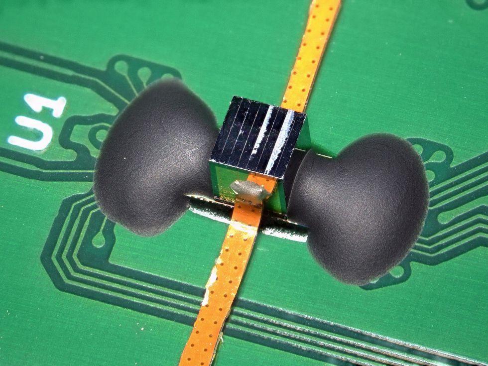
A team from University of Tokyo, Tohoku University, and the Japanese national research institute Riken explained a novel way to ease this problem at the IEEE VLSI Symposium. Instead of directly electrically connecting the bottom of the dies to the substrate, the team tested an inductive coupling transceiver system. On one side of the memory die, the team formed oblong-shaped inductive coils, about 80 by 240 µm. They placed a corresponding set at a right angle on the substrate. Current through one coil induces a magnetic field in the other, transmitting a data signal. And because the coils don’t have to overlap exactly, there’s a lot of leeway in how precisely the memory sits on the substrate.
Power connections, which are fewer in number and take up more surface area, are placed on the sides of the memory cube, University of Tokyo doctoral student Yuki Mitarai said at the symposium.
MOSAIC, which is designed to attach to the top of a GPU, fits 98 dies per cube, delivering 294 GB of memory. While it doesn’t have a microfluidic cooling structure, the fact that heat can rise through the silicon fins themselves should keep such a structure to 81.3 ℃, near today’s typical 80 ℃ limit. What’s more, thinning the DRAM dies by two-thirds to 100 µm would allow a MOSAIC cube to integrate 294 dies in the same volume, reaching 882 GB, Mitarai said.
>