Производственная платформа может обеспечить создание гибких и прозрачных фотонных чипов нового поколения
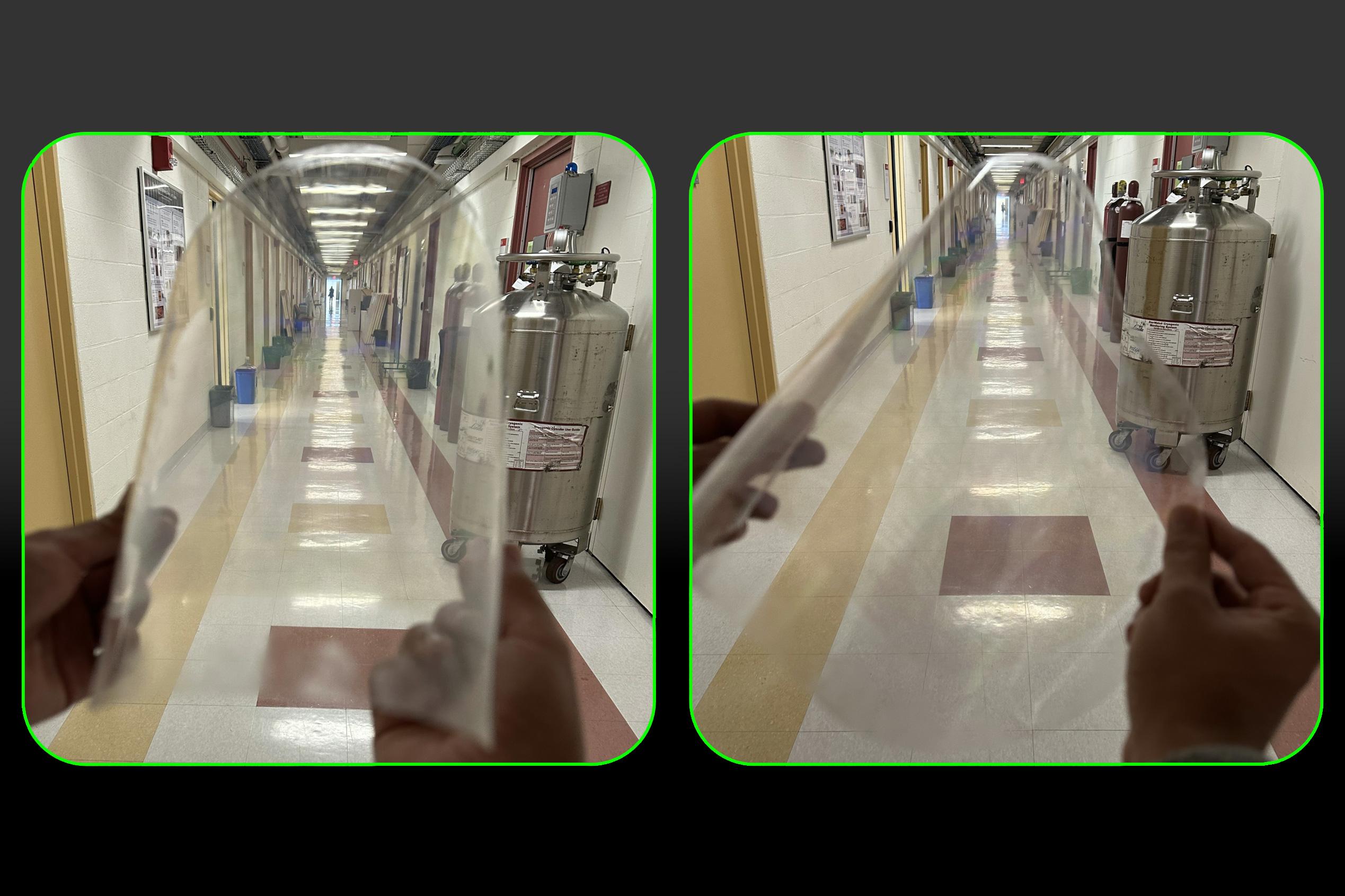
Развитие кремниевой фотоники, которая использует свет, а не электричество, для передачи и обработки данных на полупроводниковых чипах, позволило оптическим системам превратиться из громоздких устройств в компактные и усовершенствованные системы. Однако, как правило, эти кремниевые фотонные чипы жесткие и непрозрачные.
Ученые Массачусетского технологического института нашли масштабируемый способ сделать кремниево-фотонные чипы гибкими и прозрачными, что открывает путь к созданию передовых микрочипов, которые можно было бы использовать в таких приложениях, как незаметные мониторы состояния здоровья, которые адаптируются к телу, или прозрачные дисплеи дополненной реальности, которые соответствуют форме шлема пилота.
Хотя ученые недавно провели лабораторные демонстрации гибких или прозрачных чипов, они могли изготавливать только несколько устройств одновременно.
Исследователи Массачусетского технологического института в тесном сотрудничестве с инженерами из NY Creates в нанотехнологическом комплексе Олбани разработали технологический процесс, в котором используются стандартные технологии производства полупроводников для создания гибких и прозрачных кремниевых фотонных чипов на крупногабаритных пластинах.
Чтобы проверить эффективность этой платформы, исследователи тысячи раз изгибали один чип вокруг цилиндров различного диаметра — вплоть до ширины небольшого винта — без снижения производительности. Они также определили, что просмотр чипов через экран не вызовет заметного помутнения или искажения изображения.
"Сейчас мы разработали технологию производства пластин в масштабе всей пластины, которая обеспечивает механическую гибкость и оптическую прозрачность пластин, что позволяет использовать их в новых областях применения, которые ранее были невозможны при использовании кремниевой фотоники. Мы надеемся, что, тесно сотрудничая с нашими коллегами из NY Creates и используя литейный цех нанотехнологического комплекса в Олбани, у нас есть потенциал сделать платформу доступной для других групп в нашем исследовательском сообществе и открыть новые области применения в области кремниевой фотоники в целом", - говорит Елена Нотарос, доцент кафедры электротехники и компьютерных наук (EECS) Массачусетского технологического института, сотрудник исследовательской лаборатории электроники и старший автор статьи об этой технологической платформе.
Среди ее соавторов - ведущий автор Тал Снэ и Андрес Гарсия Колето, аспиранты EECS; Томас Дайер и Кевин Фили из Нью-Йоркского центра исследований, экономического развития, технологий, инженерии и науки (NY Creates); и Милика Нотарош, доктор философии, 23 года. Статья опубликована в журнале Optica.
Гибкость и прозрачность
За последнее десятилетие исследователи разработали методы для создания точных и высоконадежных устройств на основе кремниевой фотоники в больших масштабах.
Они используют передовые технологии литейного производства микроэлектроники для производства пластин диаметром 300 миллиметров с миллиардами наноразмерных оптических устройств. Но эти методы позволяют получать жесткие и непрозрачные кремниево-фотонные чипы.
"Мы поняли, что существует множество приложений, которые выиграют от использования гибкого и прозрачного чипа", - говорит Нотарос.
Scientists have previously made single silicon-photonics chips that were either transparent or flexible, but these techniques weren’t scalable. To address this scaling challenge, Notaros’ group recently demonstrated a foundry-scale process for making silicon-photonics chips on a flexible substrate.
Now, the team pushed these innovations even farther with a scalable process that produces 300-millimeter silicon-photonics wafers that are both transparent and flexible.
Their fabrication process begins as if they were making a traditional, rigid silicon wafer. The researchers carefully deposit and pattern tiny optical wires known as waveguides onto this rigid silicon substrate.
Then they bond a temporary silicon wafer on top. They flip the wafer over and remove all of the original silicon substrate from what is now the top of the wafer. They are then left with a flat layer of material with a thickness less than a tenth of a human hair.
"Thanks to the fact that we added that rigid temporary support before we flipped the wafer over, we can go all the way down so we are just left with the oxide and waveguiding layers," Sneh says.
They use an adhesive to stick a thin, transparent polyester film on top of these ultrathin layers and "de-bond" the temporary silicon wafer from the bottom to remove it.
This leaves them with a flexible, transparent wafer only a few microns thick that contains the oxide and waveguide layers needed to capture and transport light for silicon photonics.
"Because we are using stable 300-millimeter foundry fabrication tools, we can design systems with a very large number of devices and feel confident that they are going to perform up to specifications, which is extremely important," Sneh adds.
The biggest challenge in developing this fabrication process was removing enough material from a large 300-millimeter-diameter silicon wafer to leave only a few microns of material behind.
During fabrication, stress on the wafer typically causes it to bow slightly, making this silicon removal process especially challenging.
"As we were flipping the wafers over on these substrates, if the strain isn’t properly managed and the wafer isn’t perfectly flat, it is going to get ripples across its surface or even shatter in the fabrication line," Dyer says.
The researchers carefully managed that stress by sticking to low temperature processes at or below 500 degrees Celsius.
They also had to find the right ordering and combination of removal methods.
They used industrial processes to thin the silicon layer, but switched to a more precise selective chemical etch for the last bit. This ensured they would not damage the ultrathin layers left behind.
An eye on performance
The researchers performed three experiments to test different functionalities of these flexible, transparent silicon-photonics wafers.
First, they tested the optical performance of chips with integrated waveguides of different lengths to determine their waveguiding properties.
Then they tested flexibility by bending a chip thousands of times around cylinders with different diameters. These experiments showed no degradation in performance even when they bent it around a cylinder about the size of a small screw. The device didn’t start to degrade until the researchers bent it around a toothpick several times.
"This experiment validated that the platform can be used for our proposed applications, performing even well beyond the metrics required for these intended systems," Garcia Coleto says.
They also evaluated transparency by setting up a bionic eye and testing whether the chip would distort the user’s vision when placed in front of the eye. They found that the chip causes only minimal haze for the viewer and would not noticeably distort images the eye perceives when looking through it.
These characteristics could make these chips especially well-suited for enabling silicon-photonics systems for applications like curved augmented-reality displays that conform to a heads-up-display windshield or airplane pilot’s visor. In a pilot’s visor, for instance, such an augmented-reality display could replace the heavy bulk-optical systems that currently provide real-time information to help the pilot react to dangerous conditions.
In the future, the researchers want to add more complex components and functionality to the chips as they move toward enabling these and other new applications. They also want to refine the design to further improve waveguide efficiency and boost transparency performance.
This research was funded, in part, by the National Science Foundation, the U.S. Defense Advanced Research Projects Agency, and a MathWorks Fellowship. Wafer processing was performed at NY Creates, and chip dicing was conducted at MIT.nano.
>