Американские производители микросхем делают большие ставки на исследования и разработки
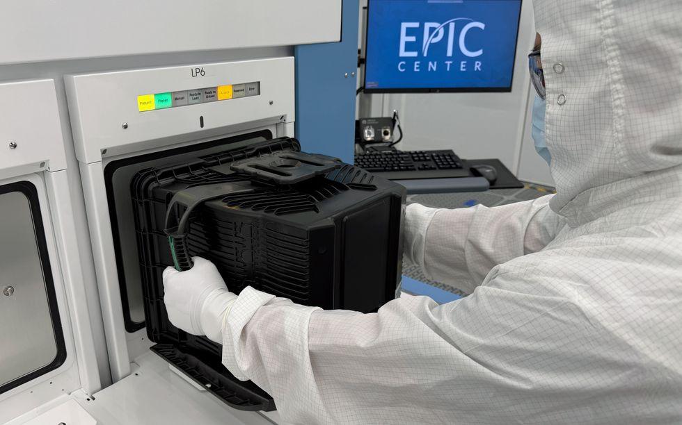
12 октября компания Applied Materials представила многомиллиардный исследовательский центр в Саннивейле, штат Калифорния, в самом сердце Кремниевой долины. В 2023 году компания впервые объявила о планах инвестировать 4 миллиарда долларов в свой центр инноваций и коммерциализации оборудования и процессов (EPIC), но теперь заявляет, что инвестирует еще больше: около 5 миллиардов долларов. Это повышение является частью более масштабного роста частных инвестиций, который одновременно расширяет сектор исследований и разработок в области полупроводников в США и делает его более сложным.
В августе две полупроводниковые компании объявили об этом грандиозном событии. Производитель чипов памяти Micron сообщил, что в течение десяти лет инвестирует 10 миллиардов долларов в свою лабораторию исследований памяти в Бойсе, штат Айдахо, а SK hynix заявила, что потратит 4 миллиарда долларов на современное упаковочное производство в Уэст-Лафайетте, штат Индиана. (Ни одна из этих компаний не ответила на вопросы IEEE Spectrum о том, какая часть этих средств будет направлена на исследования и разработки.)
Федеральное правительство США поощряет инвестиции в американские полупроводниковые исследования со стороны чип-гигантов, базирующихся в дружественных странах, таких как TSMC и Samsung. Она также ввела тарифы на иностранные компоненты и вложила часть собственных денег в слабеющие отечественные компании по производству чипов, включая Intel. Но истинная причина сегодняшней волны частных инвестиций, по мнению некоторых аналитиков и руководителей, заключается в том, что компании ожидают огромных прибылей от поддержки нынешнего безумия в области искусственного интеллекта. "Лучшее объяснение, вероятно, связано не с политикой, а с большим скачком в росте доходов, вызванным спросом на искусственный интеллект", - говорит Крис Миллер из Университета Тафтса, автор книги "Война чипов".
Деньги на ИИ, инструменты, ускоряющие производство чиповДиректор по стратегии Applied Material Тристан Холтам соглашается: "На самом деле все дело в ИИ". По оценкам фирмы, выручка десяти крупнейших полупроводниковых компаний выросла примерно на 150% с 2021 года благодаря спросу на ИИ, и они, в свою очередь, увеличили свои инвестиции в исследования и разработки на 67%, говорит он. Холтам добавляет, что в этом году ведущие полупроводниковые компании в совокупности инвестируют в исследования и разработки 67 миллиардов долларов, что значительно превышает федеральное финансирование. Большая часть этих федеральных денег поступает из2022 CHIPS and Science Act, which allocated $11 billion for R&D over several years.
While demand for AI-ready chips provides funding and motivation for more chip R&D, AI in the form of research tools is helping the people actually doing the R&D. Entegris, a semiconductor materials science company headquartered in Billerica, Mass., is applying AI in its early-stage research and design, says Olivier Blachier, the company’s Chief Innovation Officer. At his company, workers are defining performance goals for next-generation products and asking AI tools to suggest promising new materials to match. "If you’re an AI engineer, a chemist, a materials scientist, you can combine scientific understanding with AI-driven modeling and simulation to work backward from a target performance requirement," he says. The company is also piloting AI for preliminary screening of potential new materials, similar to what the pharmaceutical industry does with new molecules, before trying to synthesize and evaluate materials in the lab.
At Applied Materials, Holtam reports that the company is making use of AI-enabled acceleration in new material discovery, generative design of equipment, algorithm and software development. "The timing is perfect for EPIC," Applied Materials’s new lab devoted to equipment and processes, he declares.
An artist’s rendering depicts Applied Materials’ new, US $5 billion EPIC research center, which was opened on 12 October 2026.Applied Materials
Reshaping Chip R&D, Not Just Resizing ItPhysical proximity is emerging as a key advantage for chipmakers and that is reshaping the industry’s geographic and facilities investments. The Japanese semiconductor packaging company Resonac opened its first R&D facility in the U.S. in April, for example. "These companies have a very strong reason to want to be close to their customers and close to their customers’ customers so they can make the right investments for the next five to ten years," according to Miller.
The knowledge of how prototype chip-making equipment works does not move up and down the supply chain as easily as software. "The traditional way of working to get brand new technology into the hands of our customers, the chip makers, was to ship a prototype piece of equipment from our lab into their pilot line. That’s a kind of heart-in-your-mouth type of situation," Holtam says.
"That was always a huge point of contention," he adds. "At what level of maturity we’re willing to allow a prototype outside of our building when the chip company is pulling on that as hard as possible." Applied Material analyzed 15 years of its own internal R&D to look for the places likely to benefit from fewer such heart-stopping shipments and from more shoulder-to-shoulder lab work. Then it conducted pilot programs of its customer-in-the-lab approach and got what Holtam deemed "very, very encouraging results."
That helped prompt Applied Material to invite top customers to set up shop inside the new EPIC lab. So far, TSMC, Samsung, Micron, Broadcom, and others have said yes. Even competing customers will get their own facilities under EPIC’s roof, with digital firewalls, physical barriers, and other security features. "We’re eliminating handoffs," Holtam says, and making it easier for their own research staff to give customers a preview of what’s coming.
Applied Materials’ stated goal is for its EPIC center to reduce, by several years, the time it takes to go from early-stage discoveries to chip commercialization. That’s typically a 10-to-15 year process.
The U.S. Department of Commerce announced similar goals for big-tent semiconductor R&D facilities under the CHIPS Act, but those are now behind schedule or indefinitely paused. They might have helped startups get a leg up on the chip giants in a notoriously concentrated industry. Indeed, EPIC’s partnership announcements so far have been with other industry leaders, so startups may be at the back of the queue. Right now, generally, Blachier says, "small and medium companies have to cooperate with bigger companies to feed into the giants."
Another of the ways the industry is seeking acceleration is by closer ties with universities. Universities also serve as a bridge to the U.S. national semiconductor research strategy since universities have long-running research funding partnerships with the federal government.
"There is a benefit in having longer-term horizons and supported investments," Blachier says, referring to EU and some Asian countries’ national chip strategies, which have created successful pre-competitive research facilities such as imec. More facilities like that in the U.S., he says, would be "definitely useful, and tend to benefit the ecosystem."
>