Исследователи создают сверхтонкие сверхпроводники, устойчивые к воздействию воздуха, для более масштабируемых квантовых устройств
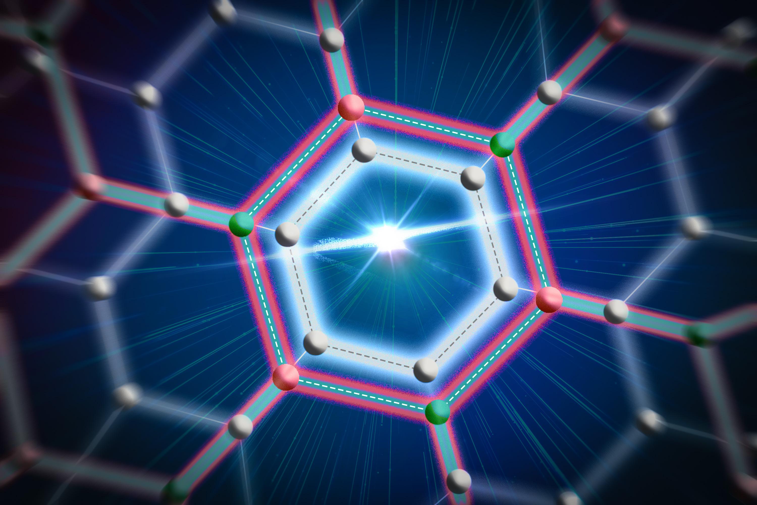
Сверхтонкие сверхпроводящие материалы толщиной всего в один или несколько атомов обладают уникальными свойствами, которые ученые могут использовать для создания более компактных, масштабируемых и эффективных квантовых устройств. Но эти хрупкие материалы так быстро разлагаются на воздухе, что их трудно изучать или изготавливать.
Теперь исследователи из Массачусетского технологического института и других организаций обнаружили и применили метод создания большой однородной области ультратонкого сверхпроводящего материала, который остается стабильным на воздухе.
Они "выращивают" сверхпроводящий материал, называемый диселенидом ниобия, под другим атомарно тонким материалом - графеном на основе углерода. Слой графена защищает хрупкий сверхпроводник от окисления, в то же время позволяя ему расти ровным слоем на большой площади пластины.
Исследователи также интегрировали этот устойчивый к воздействию воздуха сверхпроводник в сверхпроводящую микроволновую схему. При испытаниях материал сохранил свои сверхпроводящие свойства и продемонстрировал высокую кинетическую индуктивность, которая является ресурсом для многих квантовых устройств.
В долгосрочной перспективе это достижение может помочь в миниатюризации сверхпроводящего оборудования для квантовых вычислений, а также в таких технологиях, как сверхчувствительные квантовые детекторы для связи или космологии.
"Новые сверхпроводники толщиной всего в один монослой обладают большим потенциалом. Благодаря нашему новому технологическому процессу они больше не являются материалами, которые можно изготавливать только в очень небольших масштабах. Сейчас перед учеными открываются захватывающие возможности для изучения этих материалов, использования их в схемах и изучения их практического применения", - говорит один из ведущих авторов Сюйдун Шелдон Чжэн, аспирант кафедры электротехники и компьютерных наук Массачусетского технологического института (EECS).
К нему присоединились соавторы статьи Самея Заман SM ’24, аспирантка EECS, и Кенан Чжан, недавний постдок в исследовательской лаборатории электроники Массачусетского технологического института (RLE); авторы-корреспонденты Уильям Д. Оливер, профессор EECS имени Генри Эллиса Уоррена (1894) и профессор физики, директор Центра квантовой инженерии и заместитель директора RLE; Джоэл И-дж. Ван, доцент Нью-Йоркского университета; и Цзин Конг, профессор инженерных наук Массачусетского технологического института имени Джерри Макафи (1940) и член RLE; а также другие сотрудники Массачусетского технологического института и лаборатории Линкольна, Университета Райса, Йельского университета и университета Пхохан в Южной Корее. Результаты исследования опубликованы сегодня в журнале Nature.
Мощные свойства
Сверхпроводники - это материалы, которые могут проводить электричество без сопротивления, и они необходимы для некоторых типов квантовых устройств.
Двумерные сверхпроводящие материалы сохраняют свои сверхпроводящие свойства, несмотря на толщину всего в несколько атомов. Эти материалы обещают миниатюризировать сверхпроводящие схемы.
Диселенид ниобия, ультратонкий сверхпроводник, состоящий из одного плотно упакованного слоя атомов ниобия, зажатого между одним слоем атомов селена с обеих сторон, обладает оченьhigh kinetic inductance, as members of the research team recently reported.
This enables the material to store a great deal of inductive energy in a very small area. Large kinetic inductance in a small form-factor is a desirable design element in many quantum devices.
One commonly used approach to realizing a large kinetic inductance is to string together an array of devices called Josephson junctions.
If scientists could incorporate materials such as thin niobium diselenide with sufficiently large kinetic inductance into a quantum circuit, they could replace the large area of electronic junctions with a tiny piece of thin-film material, making the circuit more compact. But because niobium diselenide degrades rapidly in air, scientists have not been able to reliably fabricate devices at the wafer scale. Instead, they rely on exfoliation techniques that yield small flakes. Furthermore, researchers have struggled to grow material with uniform monolayer thickness. Consequently, it has been challenging to fully probe its properties or test it in practical applications.
"Typically, once we make the material and remove it from its inert environment, it immediately starts to oxidize and degrade, ultimately becoming damaged," Zheng explains.
Scientists usually grow niobium diselenide by depositing chemical precursors onto a silicon dioxide substrate. Then they place another layer of two-dimensional material, like graphene or hexagonal boron nitride, on top to protect the fragile superconductor from air.
But such postgrowth protection presents a challenge. The superconductor begins to oxidize almost immediately after synthesis, degrading its properties before it is protected. Meanwhile, the protection process requires a stringent inert environment and delicate processing.
Mind the gap
The MIT researchers used a different tactic. They put the layer of graphene on top of the silicon dioxide substrate first. Then they deposited the precursors and grew the superconducting material in the tiny gap between the two layers.
"It took a long time for us to understand how the growth could happen underneath the graphene. Through collaboration and discussion, we eventually uncovered the mechanism for growing the material at the interface, and this solves a lot of problems and allows us to simplify our fabrication steps," Zheng says.
The silicon dioxide substrate helps trap the precursors long enough for the crystal to begin forming, while the graphene layer allows them to move around easily and spread into a continuous monolayer.
The researchers used this technique to generate a perfectly smooth layer of niobium diselenide more than an inch in size.
"By carefully tuning the growth conditions, we can ensure the material grows between the layers in exactly the way we’ve designed," Zheng says.
Even though the graphene is placed on top of the silicon dioxide, the weak adhesion between these materials leaves a gap between them less than 1 nanometer thick. The niobium diselenide grows only within that gap. Then, since it is already encapsulated by graphene, the researchers can safely remove it into the ambient environment without causing degradation.
Careful connections
The researchers also designed an oxidation-free transfer technique to peel the graphene-niobium diselenide structure from its growth substrate, building on prior work by members of the team.
Then, they developed a method to integrate the thin film into a quantum circuit without hampering the fragile superconductor or its properties.
"It is challenging to make a good electrical connection between this very thin material, which is only about 1 nanometer in thickness, and our electrodes, which are a few hundred nanometers in thickness," Zaman says.
They carefully etch the side walls of the thin-film superconductor in a vacuum chamber, which preserves the smooth edge of the material. When they integrate the prepared niobium-graphene structure into a conventional superconducting circuit, it forms a reliable electrical connection. Importantly, the material maintained its superconducting properties and exhibited high kinetic inductance after clean room fabrication and integration into the circuit. This makes it particularly attractive for fabricating compact superconducting quantum devices and other quantum technologies.
Furthermore, the growth strategy is not limited to monolayer niobium diselenide. The researchers demonstrated that it can be extended to a broad family of monolayer quantum materials with diverse and technologically important properties.
In the future, the researchers aim to integrate these ultrathin superconducting materials into functional device architectures to enable the exploration of fundamental physics and the prototyping of quantum devices and other advanced technologies.
"We’ve taken a very good step toward exploring both the physics and the application side of this thin, monolayer superconductor, which we can now grow in wafer scale or in even larger areas. There are a lot of directions we can go in the future," Zaman says.
This research was funded, in part, by the U.S. Army Research Office, the U.S. National Science Foundation, the Schlumberger Foundation, the U.S. Department of Energy, the U.S. Air Force Office of Scientific Research, the Semiconductor Research Corporation Center, the MIT Institute for Soldier Nanotechnologies, and the National Research Foundation of Korea. This work was carried out, in part, using MIT.nano facilities.
>